Lichee Tang: The cheapest beginner FPGA
Have you ever wanted to start learning FPGAs but just can’t spare the $80-$150 for an official Xilinx/Altera board from places like Digilent? Let me introduce you to what is possibly the best beginner FPGA for learning RTL (Verilog/VHDL)!
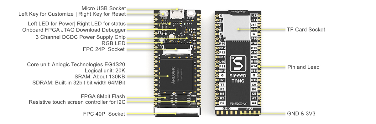
The Lichee Tang Primer is a low-cost FPGA board made by Sipeed, using Anlogic’s EG4S20BG256 FPGA. It’s a great value for money, with 20,000 LUT4 logic elements and an onboard JTAG interface for uploading your bitstreams directly to the FPGA or SPI flash. In fact, it’s vendor IDE is especially user-friendly, being able to synthesise bitstreams in a matter of seconds, instead of minutes like Quartus/Vivado from the major players.
So, what are the downsides? Firstly, it’s just not well supported by the community or industry - meaning you’ll need to learn those pesky Quartus/Vivado tools eventually if you go into industry. Secondly, you’ll need to dig through documentation to use specific features (SERDES, ADC, PLL…) and vendor-provided IP.
However, for a beginner like me, we can wait to sort out those problems later… I just want to have a cheap and user-friendly platform to learn Verilog!
To set up the toolchain for this board, you can follow the official tutorial at the Sipeed wiki. I’ll briefly go through the setup steps:
- Download the appropriate copy of Tang Dynasty IDE from Sipeed
- Download the datasheet for the board and IDE from here
- For Linux, follow the setup guidelines here and run the
td -gui command to open the IDE
- For Windows, install using the executable and set your system time to be before 2018, to enable the provided Sipeed license. Then, you will be able to run the TD IDE with the ability to synthesise the bitstream
- Install the USB drivers here
- Double-check that your setup is valid by running the Blinky example
Edit: I’ve found that Anlogic has released a new, improved version of their IDE, feel free to try it out!
Tutorial 1: FPGA Basics
As this series of tutorials were inspired by Nandland, I highly recommend you check out his videos before moving to the next few ones that actually involve implementing your designs on a physical FPGA.
For this tutorial, we will follow along with the first lecture of Nandland. Here, we will be setting up our development environment and writing a simple Verilog module and testbench with iverilog and gtkwave.
Firstly, we’ll want to install iverilog and gtkwave. iverilog is the Verilog compiler to perform simulations, and gtkwaveallows you to view the resulting waveform.
Installing iverilog and gtkwave
For Windows, download the setup executable here. Run the installer and check the “Add to PATH” option to automatically add it to PATH, allowing you to call it from the terminal. This executable also allows you to install gtkwave at the same time.
For Linux, you can install from premade packages here. Follow the instructions for your distro. For Ubuntu, add the Universe repository to your /etc/apt/sources.list and run the command sudo apt-get install iverilog gtkwave.
Setting up Visual Studio Code
I personally prefer using Visual Studio Code (VSC) as my text editor for this series, as it has some community extensions that provide linting of Verilog code. Follow this guide to install VSC, and install the extension mshr-h.veriloghdl.
After installing the extension, go to File >> Preferences >> Settings and search for Verilog.
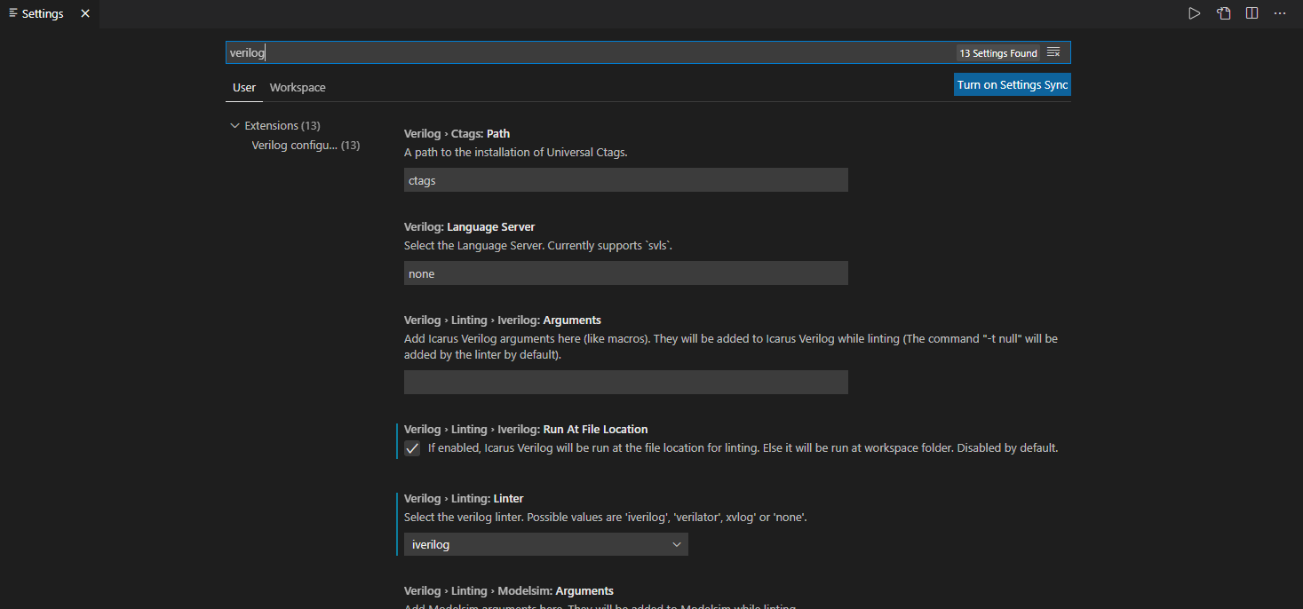
Look for Verilog >> Linting >> iverilog and check that box. Then, select iverilog as your linter of choice. This will run iverilog at your code location and dynamically provide code completion and check for syntax errors. However, this does not check for logical errors, which you will need to debug using simulation.
Module Structure
In Verilog, a module is defined with the keyword module. The following is an example of how a module is defined.
module SwitchesToLEDs
    (input i_Switch_1,
    input i_Switch_2,
    input i_Switch_3,
    input i_Switch_4,
    output o_LED_1,
    output o_LED_2,
    output o_LED_3,
    output o_LED_4);

assign o_LED_1 = i_Switch_1;
assign o_LED_2 = i_Switch_2;
assign o_LED_3 = i_Switch_3;
assign o_LED_4 = i_Switch_4;

endmodule
A module always starts with the keyword module followed by the name of the module. Following that, the input and output wires/registers to the module are defined. It’s good practice to label your variables appropriately, such as i for inputs and o for outputs. Remember to put the keyword endmodule at the end of your file.
Variables can have two main types in synthesizable Verilog: wire or reg for outputs and wire only for inputs. wire describes a physical connection between two ports, where any change in the driven state is propagated to the other side of the connection and is only compatible with combinational logic. reg is for driver states, where you can change the value of the variable using sequential logic as well.
The keyword assign can only be used with wire type variables, thereby driving the signal continuously. These will always be active, not just at the clock edge.
This example from Nandland illustrates how you can take several button inputs and directly connect them to LED outputs.
Logic Gates
Now that we’ve taken a look at this basic example, let’s try to modify it with some logic gates.
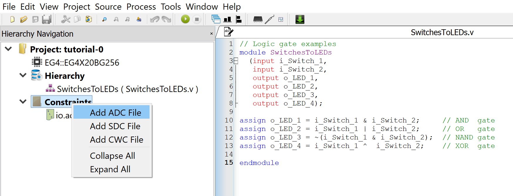
// Logic gate examples
module SwitchesToLEDs
    (input i_Switch_1,
    input i_Switch_2,
    output o_LED_1,
    output o_LED_2,
    output o_LED_3,
    output o_LED_4);

assign o_LED_1 = i_Switch_1 & i_Switch_2;     // AND  gate
assign o_LED_2 = i_Switch_1 | i_Switch_2;     // OR   gate
assign o_LED_3 = ~(i_Switch_1 & i_Switch_2);  // NAND gate
assign o_LED_4 = i_Switch_1 ^  i_Switch_2;    // XOR  gate

endmodule
In this example, we use the bitwise operators &, |, ~ and ^ for AND, OR, NOT and XOR. It is also possible to use full logical operators such as &&, || and ! for AND, OR and NOT. A deep dive into operators is available here.
Creating a Testbench for Simulation
Now, let’s save our file as SwitchesToLEDs.v. Create a new file for our testbench called SwitchesToLEDs_tb.v. At the start of the file, we will define the timescale for which the simulation is done over, which is the duration of one clock pulse.
Following that, we will need to include the source Verilog file of our module.
`include "SwitchesToLEDs.v"
Then, we will create our testbench module. Testbenches don’t contain inputs or outputs, hence there are no brackets containing them.
`timescale 1ns/1ns
`include "SwitchesToLEDs.v"

module SwitchesToLEDs_tb;
	// Code for testbench here
endmodule
Now we create the inputs and outputs for our module, which we call the Unit Under Test (UUT). reg for inputs and wire for outputs, the reverse of what we declared in the actual module. This allows us to drive the inputs and read the outputs of the UUT.
`timescale 1ns/1ns
`include "SwitchesToLEDs.v"

module SwitchesToLEDs_tb;
    reg i_Switch_1;
    reg i_Switch_2;
    wire o_LED_1;
    wire o_LED_2;
    wire o_LED_3;
    wire o_LED_4;

    // Code for testbench here
endmodule
Next, we instantiate the UUT. When instantiating a module, the format is moduleName (parameters) InstanceName (inputs/outputs). You can provide the inputs/outputs in order, or you can use their internal variable names to match them, as shown below.
`timescale 1ns/1ns
`include "SwitchesToLEDs.v"

module SwitchesToLEDs_tb;
    reg i_Switch_1;
    reg i_Switch_2;
    wire o_LED_1;
    wire o_LED_2;
    wire o_LED_3;
    wire o_LED_4;

    // Instantiating module to test
    SwitchesToLEDs uut(
        .i_Switch_1(i_Switch_1),
        .i_Switch_2(i_Switch_2),
        .o_LED_1(o_LED_1),
        .o_LED_2(o_LED_2),
        .o_LED_3(o_LED_3),
        .o_LED_4(o_LED_4)
    );
    // Code for testbench here
endmodule
Now, let’s initialise the testbench procedure that we want to conduct. The initial keyword allows us to define behaviour that only happens once, at the beginning. Verilog doesn’t use curly braces to detect code blocks, rather it uses begin and end keywords.
To output the simulated values of all testbench variables, use the command $dumpfile() and $dumpvars() to save them into a vcd format readable by gtkwave.
`timescale 1ns/1ns
`include "SwitchesToLEDs.v"

module SwitchesToLEDs_tb;
	reg i_Switch_1;
    reg i_Switch_2;
    wire o_LED_1;
    wire o_LED_2;
    wire o_LED_3;
    wire o_LED_4;

    // Instantiating module to test
    SwitchesToLEDs uut(
    	.i_Switch_1(i_Switch_1),
        .i_Switch_2(i_Switch_2),
        .o_LED_1(o_LED_1),
        .o_LED_2(o_LED_2),
        .o_LED_3(o_LED_3),
        .o_LED_4(o_LED_4)
    );

    initial begin
    	// Define testbench behaviour
        $dumpfile("SwitchesToLEDs_tb.vcd");
        $dumpvars(0, SwitchesToLEDs_tb);

        // Code for testbench here
    end

endmodule
Since we want to test our AND, OR, NAND and XOR gate behavior, let’s create a truth table for the expected outputs for every given set of inputs. For simplicity, let’s call the switches A and B respectively, and outputs C, D, E, F.
| A |
B |
C |
D |
E |
F |
| 0 |
0 |
0 |
0 |
1 |
0 |
| 1 |
0 |
0 |
1 |
1 |
1 |
| 0 |
1 |
0 |
1 |
1 |
1 |
| 1 |
1 |
1 |
1 |
0 |
0 |
Setting these inputs respectively, with a delay of 10 timesteps using #10 in the testbench. The curly bracket notation groups signals into buses from left to right, Most Significant Bit to Least Significant Bit.
`timescale 1ns/1ns
`include "SwitchesToLEDs.v"

module SwitchesToLEDs_tb;
	reg i_Switch_1;
    reg i_Switch_2;
    wire o_LED_1;
    wire o_LED_2;
    wire o_LED_3;
    wire o_LED_4;

    // Instantiating module to test
    SwitchesToLEDs uut(
    	.i_Switch_1(i_Switch_1),
        .i_Switch_2(i_Switch_2),
        .o_LED_1(o_LED_1),
        .o_LED_2(o_LED_2),
        .o_LED_3(o_LED_3),
        .o_LED_4(o_LED_4)
    );

    initial begin
    	// Define testbench behaviour
        $dumpfile("SwitchesToLEDs_tb.vcd");
        $dumpvars(0, SwitchesToLEDs_tb);

        // Test conditions
        {i_Switch_1, i_Switch_2} = 2'b00; #10;
        {i_Switch_1, i_Switch_2} = 2'b10; #10;
        {i_Switch_1, i_Switch_2} = 2'b01; #10;
        {i_Switch_1, i_Switch_2} = 2'b11; #10;
    end

endmodule
Knowing that our test cases are sequentially incrementing, we can use a for loop using an integer variable. However, keep in mind that these constructs are not synthesizable and cannot be used in your main module. Keep in mind that ++ is not valid to increment your counter. Use $display() to print messages to terminal.
`timescale 1ns/1ns
`include "SwitchesToLEDs.v"

module SwitchesToLEDs_tb;
	reg i_Switch_1;
    reg i_Switch_2;
    wire o_LED_1;
    wire o_LED_2;
    wire o_LED_3;
    wire o_LED_4;

    // Instantiating module to test
    SwitchesToLEDs uut(
    	.i_Switch_1(i_Switch_1),
        .i_Switch_2(i_Switch_2),
        .o_LED_1(o_LED_1),
        .o_LED_2(o_LED_2),
        .o_LED_3(o_LED_3),
        .o_LED_4(o_LED_4)
    );

    initial begin
    	// Define testbench behaviour
        $dumpfile("SwitchesToLEDs_tb.vcd");
        $dumpvars(0, SwitchesToLEDs_tb);

        // Test conditions
        for (integer i=0; i<4; i = i+1) begin
        	{i_Switch_1, i_Switch_2} = i;
            #10;
        end

        $display("Test completed!");
    end

endmodule
With this, we have finished our Verilog testbench. To run it and generate the vvp file, use the following command:
iverilog -o SwitchesToLEDs_tb.vvp SwitchesToLEDs_tb.v
Then, create the output vcd file.
vvp SwitchesToLEDs_tb.vvp
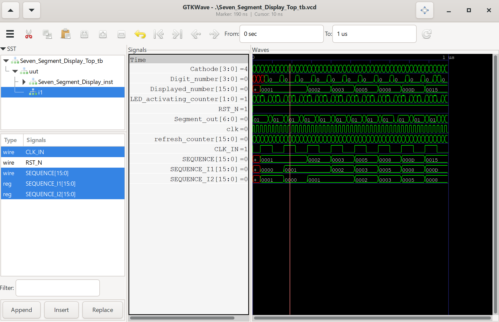
Now, let’s open gtkwave by typing that in a terminal, bringing up the GUI. Click on File >> Open New Tab and find your .vcd output file.
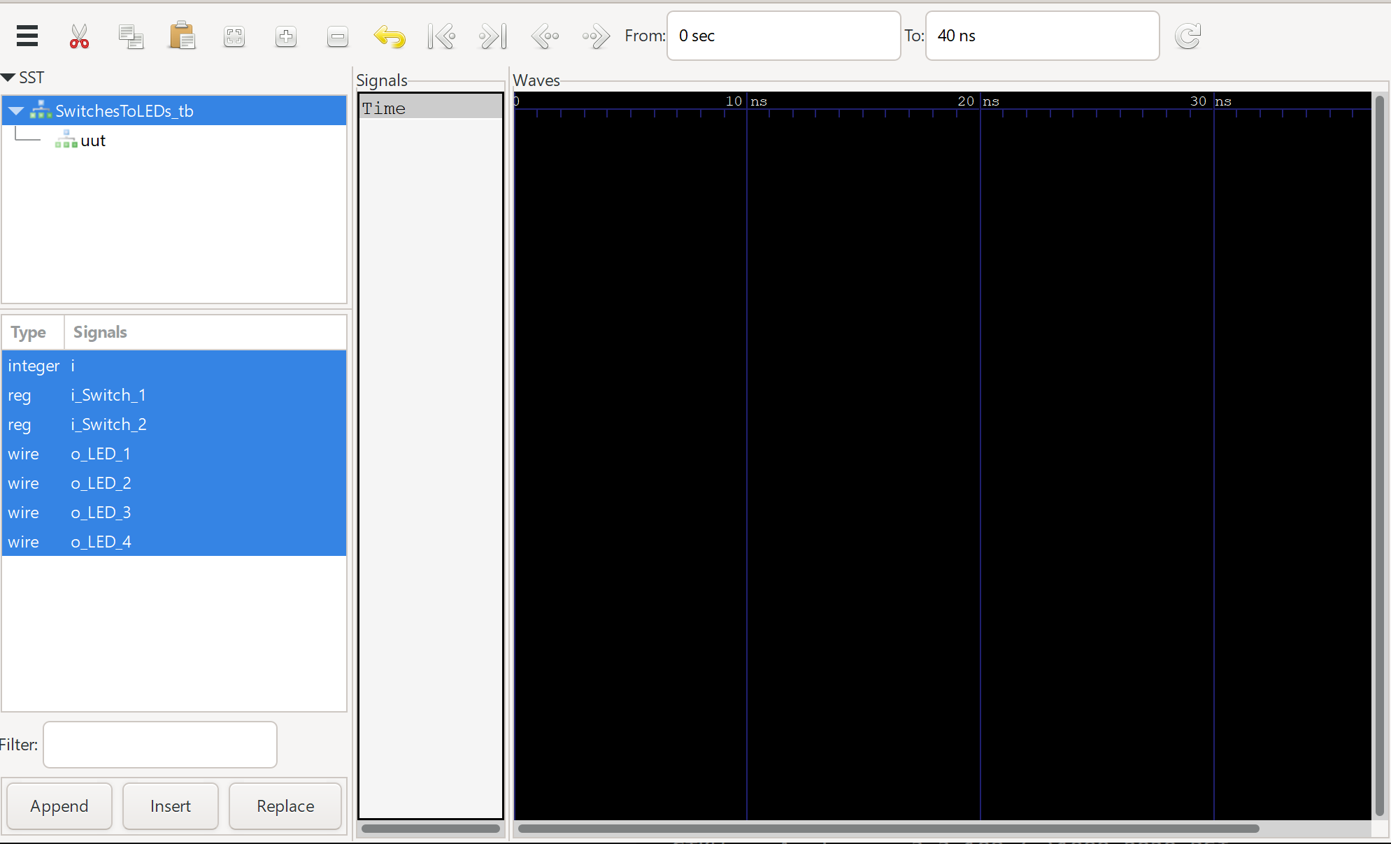
Select all your signals by clicking on the top one, then Shift+click on the bottom to select all. Click Append to add them to the waveform viewer.
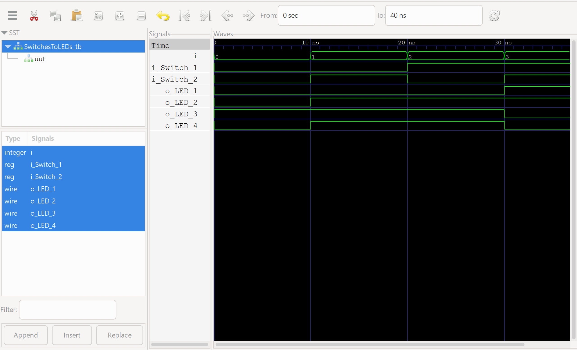
Comparing the result of our waveforms to the truth table, we see that everything is working fine! Look horizontal across the truth table and vertical down the waveform for a 1:1 comparison in this case.
Deploying to hardware
Now that we know our program works fine with the simulator, let’s deploy it on actual hardware! Open up the Tang Dynasty IDE using either td -gui in Linux or through your TimeAsDate program in Windows.
Right-click the Project menu and click on New Project.
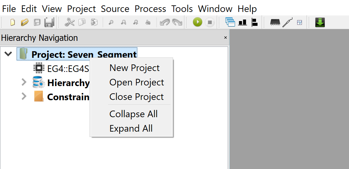
Select the correct device name for the board, EG4X20BG256.
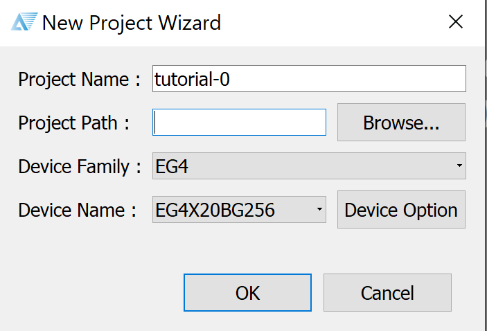
If you’ve saved your Verilog source file in the same directory, you can click Add Sources to add your source file to the project. If not, click New Source and paste in your Verilog code from SwitchesToLEDs.v.
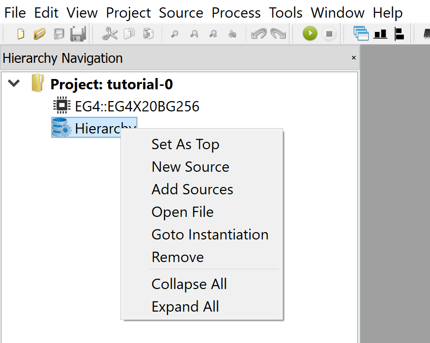
The IDE will automatically set your only source file as the Top module. In a Verilog design, the project starts from the Top module, which contains instantiations of all other modules in the hierarchy. We’ll touch on this in a later tutorial where we combine multiple Verilog source files into a single design.
Now, we’ve got to define our Constraints file, which defines how these pins are connected to external I/O on the FPGA. In your text editor, create a file called io.adc and save it with the following contents. LOCATION defines the external pin, IOSTANDARD defines the voltage logic levels and DRIVESTRENGTH defines the current driver strength in mA.
set_pin_assignment	{ i_Switch_1 }	{ LOCATION = A4; IOSTANDARD = LVCMOS33; }
set_pin_assignment	{ i_Switch_2 }	{ LOCATION = A3; IOSTANDARD = LVCMOS33; }
set_pin_assignment	{ o_LED_1 }	{ LOCATION = C5; IOSTANDARD = LVCMOS33; DRIVESTRENGTH = 20; }
set_pin_assignment	{ o_LED_2 }	{ LOCATION = B6; IOSTANDARD = LVCMOS33; DRIVESTRENGTH = 20; }
set_pin_assignment	{ o_LED_3 }	{ LOCATION = C9; IOSTANDARD = LVCMOS33; DRIVESTRENGTH = 20; }
set_pin_assignment	{ o_LED_4 }	{ LOCATION = B10; IOSTANDARD = LVCMOS33; DRIVESTRENGTH = 20; }
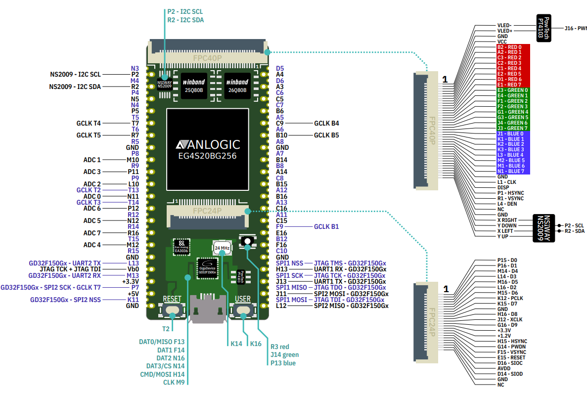
If you are making your own connections, refer to the schematic for the correct LOCATION.
Right-click Constraints and Add ADC File.
Now, double click on Generate Bitstream to start the whole process of synthesis, place-and-route, and implementation. Alternatively, you can step through this process one at a time.
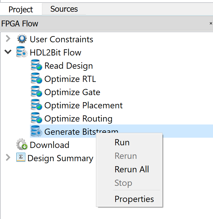
This will generate a .bit file, the bitstream to be uploaded to the board. Double-click on Download and Add the file. Click Run to upload the file directly to the FPGA. As the FPGA fabric is volatile, it will lose its configuration when powered off. To keep it, you will need to Create Flash File and upload that file to the flash instead. We won’t be covering that here as it’s not immediately useful for learning purposes. You should see the same behaviour observed in your simulation.
Congratulations! You’ve done your first FPGA project and you’re well on your way down a rabbit hole of programmable logic fun!
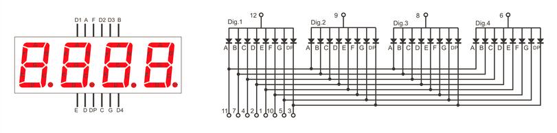
Tutorial 2: Seven Segment Display
In this tutorial, we will control a seven segment display using the FPGA. This will introduce concepts such as module instantiation where code can be written and reused, a similar paradigm to Object Oriented Programming. Click here for the tutorial.
Tutorial 3: UART Interface
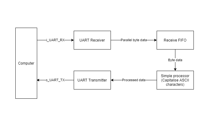
In this tutorial, we will create a UART interface to send and receive data with your computer. This introduces a state machine to handle incoming data, and how to break down complex logic into states for easier management. Click here for the tutorial.
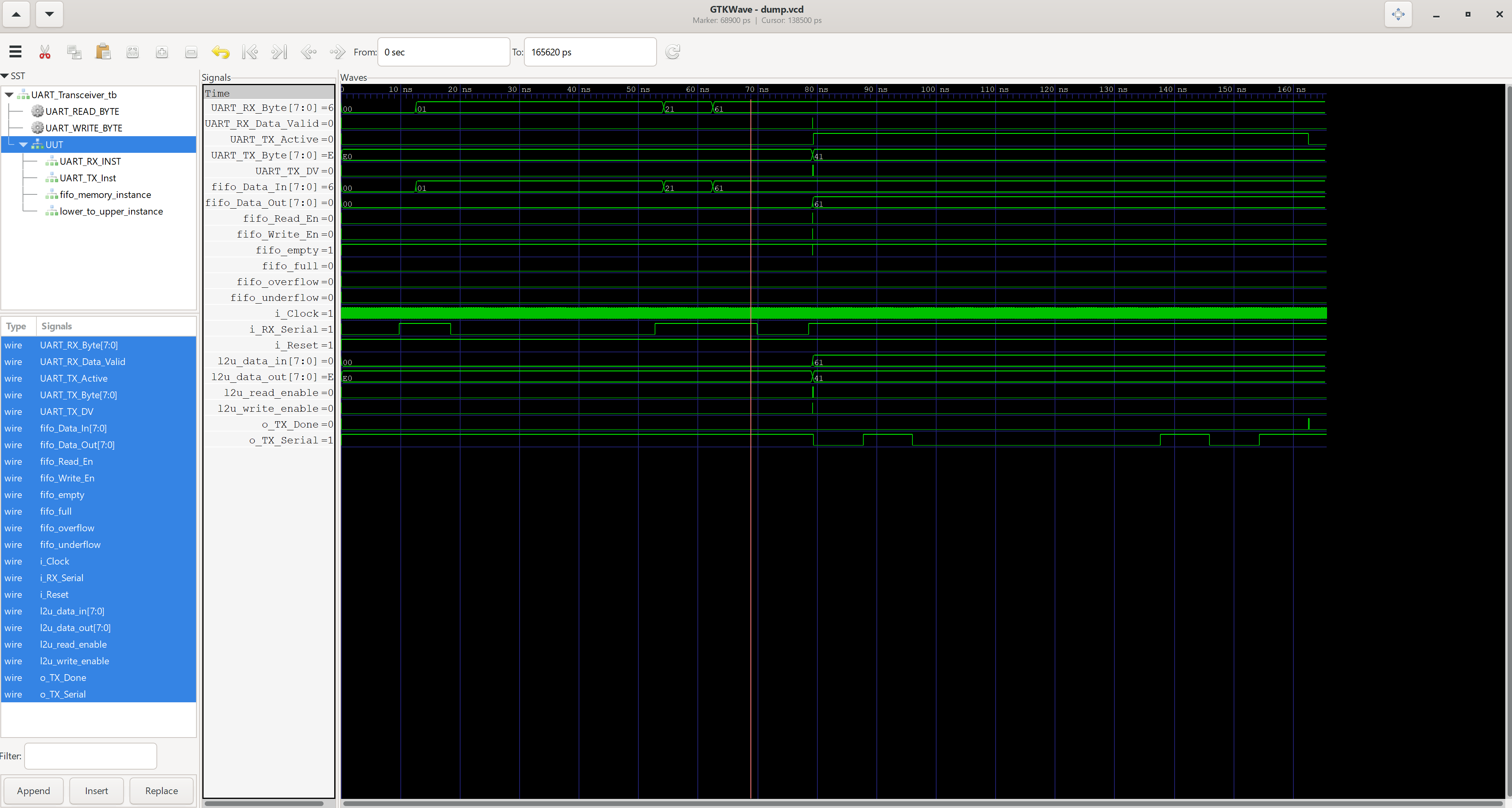
Tutorial 4: FIFO Buffer
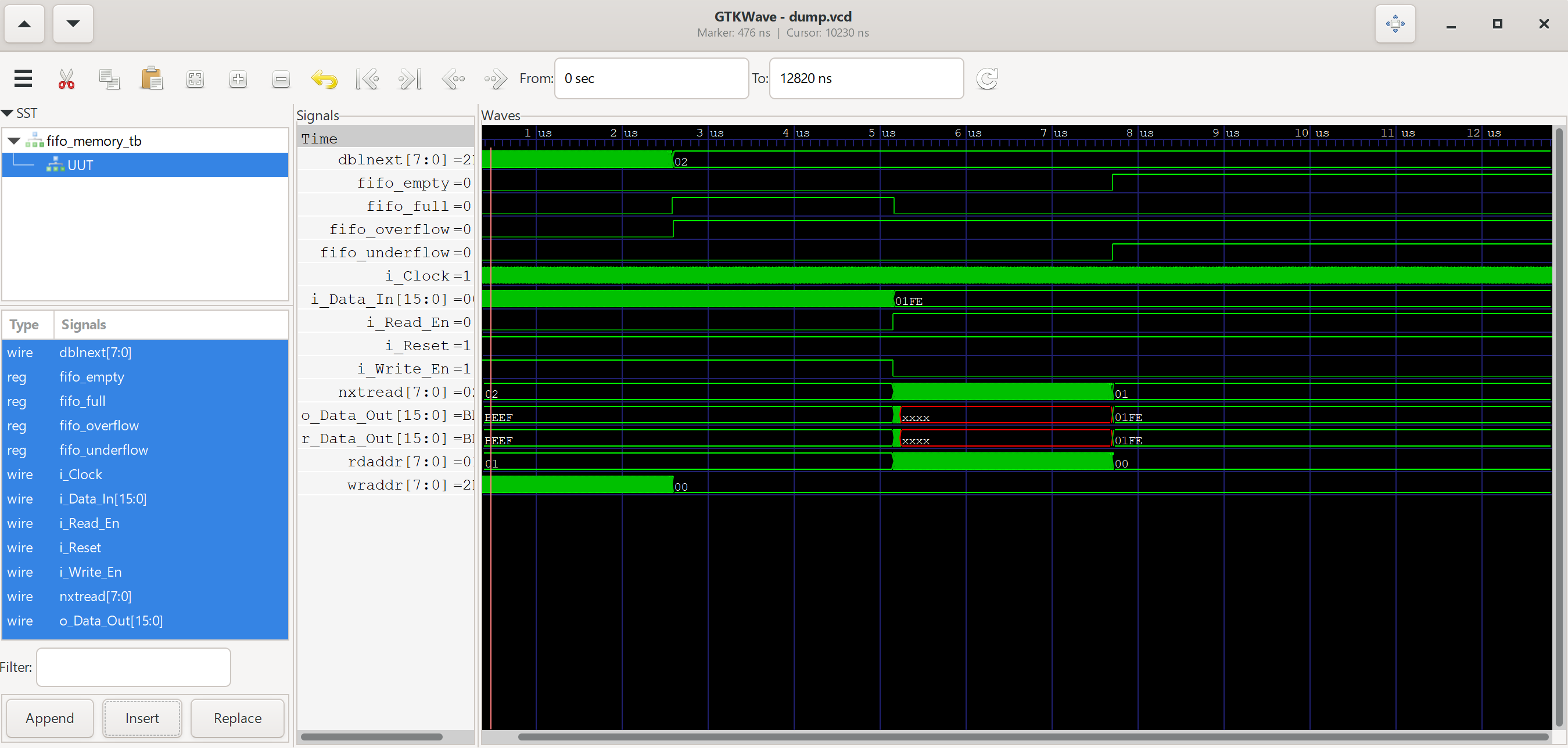
This introduces the concept of a First In First Out (FIFO) buffer between the external UART interface and the internal FPGA logic. This is necessary as the UART peripheral and internal FPGA logic work in different clock domains, and may not always be available to receive data when it is transmitted/received. Click here for the tutorial.
Tutorial 5: VGA Interface
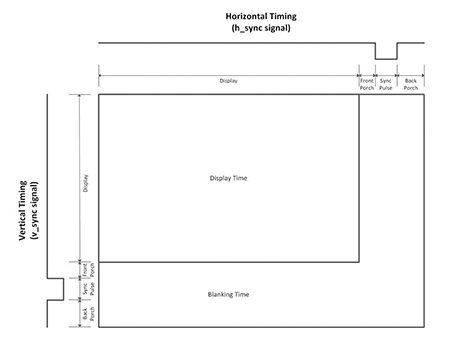
In this tutorial, we will explore the VGA specification to send RGB video data out to a monitor. This should work with any old or modern monitor. Modern monitors may rescale your image to fit the 16:9 aspect ratio. Click here for the tutorial.
Tutorial 6: HDMI Interface
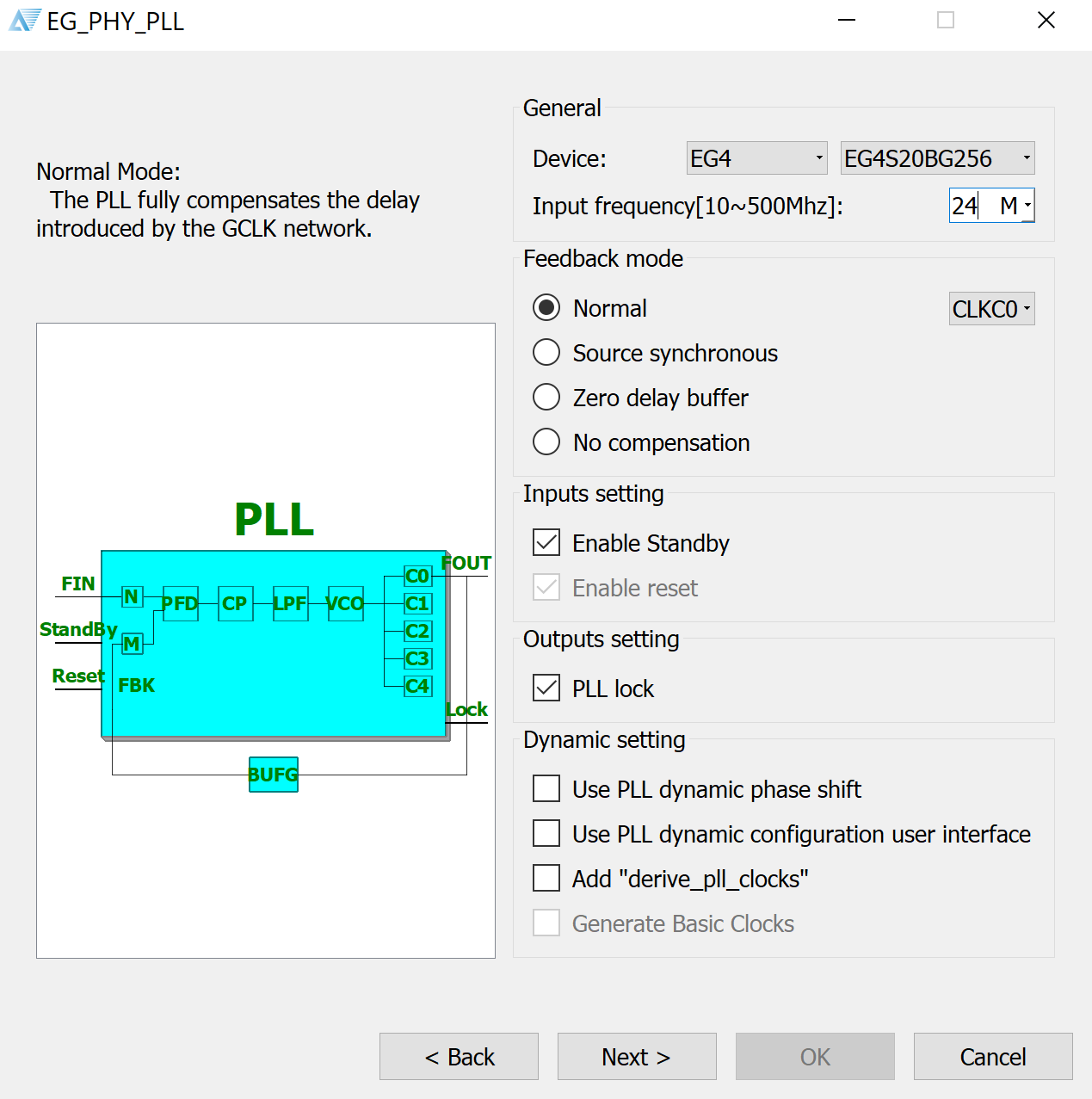
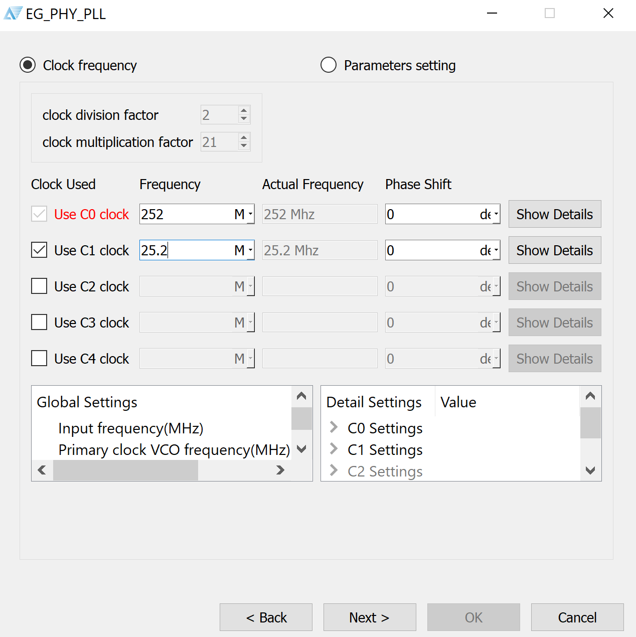
This expands on the previous tutorial to send RGB video data out to a monitor through HDMI. DVI/HDMI demands much higher clock speeds, and this is where we introduce the concept of a Phase Locked Loop (PLL), to generate faster clock signals. Click here for the tutorial.
References
For this tutorial I referenced the following sources:
 31 Jul 2021 - Jeremy See